描述
| Maximum rated values | ||||||||||||||||||||
| Definition | Symbol | Conditions | Value | Unit | ||||||||||||||||
| Supply voltage VCC | VSUP | 15.5 | V | |||||||||||||||||
| Logic input voltage | VIN_A/B | 15.5 | V | |||||||||||||||||
| Gate peak current | IOUT | ±8 | А | |||||||||||||||||
| Frequency PWM | fSW | Gate charge QG = 5600 uC | 15 | kHz | ||||||||||||||||
| Isolation voltage | VISOL | First to second side, 2 sec | 4000 | V rms | ||||||||||||||||
| Output power | POUT | For 1 chanel | 2 | W | ||||||||||||||||
| dV/dt | dV/dt | Rate of change of input to output voltage |
50 | kV/μs | ||||||||||||||||
| DC-link voltage | VDC | 1100 | V | |||||||||||||||||
| Collector-Emitter voltage | VCE | 1700 | V | |||||||||||||||||
| Operating temperature | TOP | -40..+85 | °C | |||||||||||||||||
| Storage temperature | TSTOR | -40..+85 | °C | |||||||||||||||||
| Characteristics | ||||||||||||||||||||
| Definition | Symbol | Conditions | Value | Unit | ||||||||||||||||
| min. | typ. | max. | ||||||||||||||||||
| Supply voltage VCC | VSUP | 14.5 | 15 | 15.5 | V | |||||||||||||||
| UVLO threshold | VUVLO | Switch-off threshold 13.7 V Switch-on threshold 14.3 V |
13.7 | 14.3 | V | |||||||||||||||
| Supply current ICC | Is(idle) | Without load | 80 | mA | ||||||||||||||||
| Average supply current | Is(max) | fSW= 15 kHz QG= 5600 μC | 390 | mA | ||||||||||||||||
| Turn-on threshold | V(on) | Amplitude of control signals 15 V | 8.2 | V | ||||||||||||||||
| Turn-off threshold | V(off) | 6.4 | V | |||||||||||||||||
| Input resistance switching channels | RIN(sw) | 3 | kΩ | |||||||||||||||||
| Control channel input capacity | CIN(sw) | 100 | pF | |||||||||||||||||
| Turn-on delay | td(on) | 250 | ns | |||||||||||||||||
| Turn-off delay | td(off) | 250 | ns | |||||||||||||||||
| Dead time | tIDT | Half-bridge mode | 3.2 | us | ||||||||||||||||
| Input resistance F out A/B channels | RIN_F(A), RIN_F(B), |
4.7 | kΩ | |||||||||||||||||
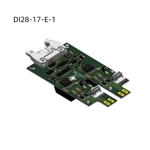
| Plug & play IGBT gate driver datasheet | ||||||||||||||||||||
| Turn-on output voltage | VG(on) | 15 | V | |||||||||||||||||
| Turn-off output voltage | VG(off) | -9 | V | |||||||||||||||||
| VCE monitoring threshold | VCE(ref) | 8.2 | V | |||||||||||||||||
| Response time | tbl(VCE) | 8 | us | |||||||||||||||||
| Turn-on gate resistor | RG(on) | 1 | Ω | |||||||||||||||||
| Turn-off gate resistor | RG(off) | 1 | Ω | |||||||||||||||||
| Creepage distance primary to secondary side | lclear(PS) | 7.7 | mm | |||||||||||||||||
| Creepage distance secondary to secondary side |
lclear(SS) | 5.8 | mm | |||||||||||||||||
| Weight | W | 34.2 | g | |||||||||||||||||
| Operating mode « F out» The driver is in a working state if the output of the contact «F out» is logical 1 (+15). If the contact output contains F out logic 0 (0 V), the driver is in an error state for one or more of the following reasons: 1. Channel A is in error. 2. Channel B is in error. 3. Driver supply voltage below minimum (+13.7 V) Operating mode “F out A / B” Selects the level of the Signal A / B control input signals Operation mode selection Operating mode of UVLO DESAT circuit mode |
||||||||||||||||||||